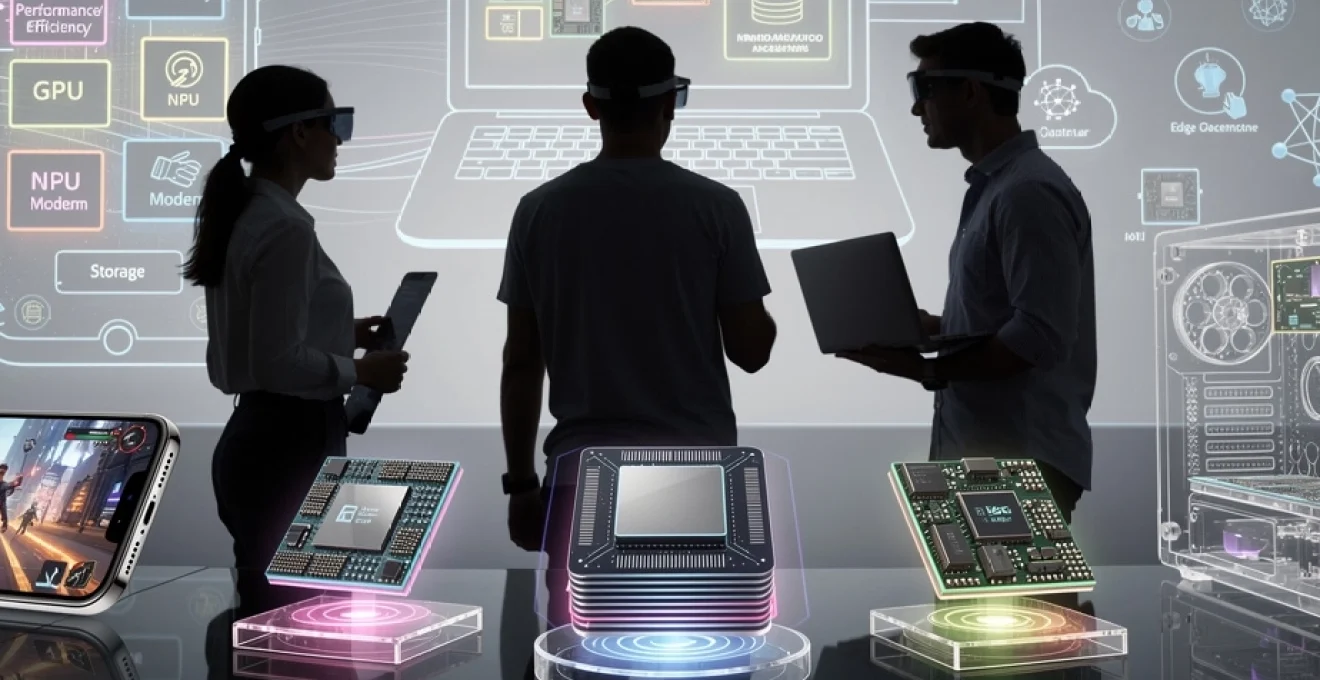
The landscape of computing has shifted dramatically over the past decade, driven by relentless innovation in microprocessor design. Today’s advanced processors represent far more than incremental improvements—they embody fundamental architectural reimaginings that enable capabilities previously confined to science fiction. From smartphones that perform real-time language translation to laptops that accelerate artificial intelligence workloads locally, these silicon marvels have become the cornerstone of technological progress. The convergence of heterogeneous computing, specialized accelerators, and cutting-edge manufacturing processes has created a new paradigm where devices adapt intelligently to diverse workloads whilst consuming minimal power. Understanding these architectural innovations isn’t merely an academic exercise; it’s essential knowledge for anyone navigating the rapidly evolving technology landscape, whether you’re selecting hardware for professional workflows or simply trying to comprehend why your next device performs so differently from its predecessor.
ARM Cortex-X4 and apple M3: architectural innovations driving mobile and desktop performance
The competition between ARM-based architectures and Apple’s proprietary silicon has fundamentally reshaped expectations for what mobile and desktop processors can achieve. These processors demonstrate that raw clock speed no longer dictates performance—instead, sophisticated architectural choices, intelligent power management, and task-specific accelerators define capability. The latest generation of these chips delivers performance that rivals traditional desktop processors whilst fitting within the thermal and power constraints of fanless designs, a feat that seemed impossible just five years ago.
Armv9 instruction set architecture and SVE2 vector extensions
The ARMv9 instruction set architecture represents a generational leap from its predecessor, introducing Scalable Vector Extension 2 (SVE2) that dramatically enhances parallel processing capabilities. Unlike fixed-width vector instructions, SVE2 allows implementations to scale from 128-bit to 2048-bit vector lengths, providing unprecedented flexibility for different workload types. This architecture particularly excels in machine learning inference, digital signal processing, and computational photography—tasks that define modern smartphone experiences. The variable-length vectors enable developers to write code once that optimally executes across different processor implementations, from budget smartphones to flagship devices, without performance compromises.
ARM’s Cortex-X4 core, built on ARMv9, pushes single-threaded performance to new heights whilst maintaining the power efficiency ARM architectures are renowned for. The core features a substantially wider execution pipeline with improved branch prediction accuracy exceeding 95%, reducing the performance penalties from mispredicted branches that plague traditional architectures. This design philosophy—combining wider execution resources with smarter predictive logic—delivers approximately 15% higher performance per clock cycle compared to previous generations, enabling smartphone processors to genuinely rival laptop-class performance in many scenarios.
Apple silicon’s unified memory architecture and neural engine integration
Apple’s M3 processor family exemplifies a different architectural philosophy entirely, one that prioritises tight integration and unified memory access over modular flexibility. The unified memory architecture allows the CPU, GPU, Neural Engine, and other specialized accelerators to access the same memory pool without costly data transfers between separate memory hierarchies. This approach eliminates the traditional bottleneck where data must be copied from system RAM to GPU memory, dramatically accelerating workflows involving large datasets or frequent hand-offs between processing units. Video editors working with 8K footage experience this advantage directly—effects that previously required rendering now play back in real-time because the GPU instantly accesses footage processed by the CPU.
The Neural Engine integrated into M3 processors handles up to 18 trillion operations per second, specifically optimized for the matrix multiplication and convolution operations that underpin modern machine learning models. Unlike general-purpose GPU compute, this dedicated accelerator executes AI workloads with superior energy efficiency, enabling features like real-time background removal in video calls or intelligent photo enhancement without noticeably impacting battery life. This specialization reflects a broader industry trend: as certain computational patterns become ubiquitous, dedicating silicon real estate to them proves more efficient than relying on programmable but less optimized general-purpose cores.
TSMC N3B process node: transistor density and power efficiency gains
Manufacturing process technology directly influences what processor architectures can achieve, and TSMC’s N3B (3-nanometer class) process node represents the cutting edge of commercial semiconductor fabrication. This process packs approximately 300
million transistors per square millimetre, enabling significantly more complex logic and larger caches in the same die area. Compared to 5 nm-class nodes, N3B typically delivers 15–18% performance gains at the same power, or up to 30% power savings at equivalent performance, depending on the voltage and frequency targets. For end users, this translates into tangible benefits: thinner devices that stay cooler under load, laptops that sustain high performance for longer without throttling, and smartphones that deliver console-class gaming without burning through battery in an hour. At scale, the cumulative energy savings across millions of devices also have meaningful implications for data centre efficiency and environmental impact.
The tighter transistor geometry of N3B also improves signal integrity and reduces leakage currents, which are crucial for always-on features such as background AI inference and secure enclaves. However, designing for such advanced nodes introduces new challenges: engineers must contend with increased variability, stricter design rules, and soaring fabrication costs. This is why we see advanced process nodes reserved for flagship SoCs like Apple’s M3 and top-tier mobile chipsets, while mid-range devices continue to rely on more mature, cost-effective nodes. As manufacturing techniques mature and yields improve, we can expect 3 nm-class technology to filter down the product stack, making next-generation performance more accessible.
Heterogeneous computing with performance and efficiency core clusters
Both ARM Cortex-X4-based designs and Apple’s M3 family rely heavily on heterogeneous computing, combining clusters of performance (P) cores and efficiency (E) cores. Instead of treating the processor as a uniform pool of identical cores, this approach assigns latency-sensitive, bursty workloads to high-performance cores while routing background tasks and lightweight threads to energy-efficient ones. Think of it as a workforce where specialists handle complex, time-critical projects and generalists quietly keep routine operations running in the background. The result is a system that feels responsive under load yet sips power when idling or handling basic tasks.
In practice, this heterogeneous microprocessor design requires sophisticated scheduling algorithms and operating system support. Apple’s macOS and iOS, for example, use advanced heuristics and telemetry to predict which tasks deserve P-core time, while Android partners leverage ARM’s DynamIQ and vendor-specific schedulers. For you as a user, the benefit is subtle but profound: your device wakes instantly, launches apps quickly, and still achieves all-day battery life. For developers, optimising software to be multi-threaded and aware of heterogeneous resources becomes a key differentiator, especially for workloads like video editing, 3D rendering, and mobile gaming that can span CPU, GPU, and NPU resources simultaneously.
Qualcomm snapdragon 8 gen 3 and MediaTek dimensity 9300 in 5g-enabled smartphones
In the smartphone arena, Qualcomm’s Snapdragon 8 Gen 3 and MediaTek’s Dimensity 9300 exemplify how advanced microprocessors enable premium 5G devices to double as pocket-sized workstations. These SoCs blend cutting-edge CPU clusters, powerful GPUs, dedicated NPUs, and integrated 5G modems into a single package, optimised for tight thermal envelopes. The focus is no longer just on benchmarking scores; instead, it is on sustained performance, on-device AI, and immersive media experiences. As we move into a world where phones handle AI image generation, real-time translation, and console-grade games, the balance of performance per watt becomes critical.
Interestingly, Snapdragon 8 Gen 3 and Dimensity 9300 adopt different philosophies to reach similar goals. Qualcomm retains a mix of performance and efficiency CPU cores, while MediaTek’s Dimensity 9300 famously goes all-in on performance cores, banking on architectural efficiency and advanced process nodes to keep power in check. For power users, this translates into smoother multitasking and faster content creation workflows. For developers, these platforms provide a rich playground of APIs—ranging from Vulkan and ray tracing extensions to AI SDKs—that help unlock the full potential of next-generation smartphone microprocessors.
Integrated X75 modem and mmwave antenna array optimisation
The Snapdragon X75 modem, integrated with Snapdragon 8 Gen 3, illustrates how modern microprocessors extend far beyond core compute. By tightly coupling the 5G modem with the application processor, Qualcomm reduces latency, improves power management, and enables smarter scheduling of data-intensive tasks such as cloud gaming and 4K streaming. The X75 supports both sub-6 GHz and mmWave 5G, combining up to 10-carrier aggregation and advanced beamforming to maximise bandwidth even in congested urban environments. For users, this means faster downloads, lower latency video calls, and more consistent performance in challenging radio conditions.
mmWave, while offering extraordinary peak speeds, demands meticulous antenna array optimisation. Smartphone designers must integrate multiple antenna modules around the chassis to compensate for signal blockage by the user’s hand or body. Here, built-in AI routines within the modem and SoC dynamically adjust beam steering and power levels based on how you hold the device and your movement patterns. It’s akin to a constantly adapting radar system, quietly working to keep your connection stable as you move through the world. Of course, these capabilities rely on careful co-design between silicon, RF front-end components, and system software, underscoring the interdisciplinary nature of modern mobile processor design.
Adreno 750 GPU architecture for ray tracing and HDR gaming
The Adreno 750 GPU in Snapdragon 8 Gen 3 brings hardware-accelerated ray tracing and advanced HDR rendering into the mainstream mobile gaming ecosystem. Ray tracing, once confined to high-end PCs and consoles, simulates realistic lighting, reflections, and shadows by tracing the paths of individual rays of light. On a constrained mobile power budget, this is a formidable challenge, but Adreno’s tiled rendering architecture and dedicated ray tracing units make it manageable. In practical terms, you get more lifelike reflections in water or glass and more nuanced lighting in complex scenes—all while maintaining playable frame rates.
Beyond eye candy, the Adreno 750 emphasises energy-efficiency and sustained performance. Intelligent workload distribution, dynamic frequency scaling, and improved shader execution efficiency ensure that longer gaming sessions do not immediately trigger thermal throttling. If you develop mobile games or VR applications, tapping into these GPU capabilities via modern graphics APIs like Vulkan and OpenGL ES can dramatically enhance visual fidelity without sacrificing responsiveness. The combination of ray tracing, variable rate shading, and high-refresh-rate displays effectively turns next-generation smartphones into handheld consoles, blurring the lines between mobile and traditional gaming platforms.
Hexagon NPU accelerators for on-device AI inference and computer vision
Qualcomm’s Hexagon NPU in Snapdragon 8 Gen 3 is purpose-built for on-device AI inference, handling tasks such as image enhancement, voice recognition, and generative AI. Rather than offloading everything to the cloud, these accelerators run models locally, reducing latency and preserving privacy. Hexagon’s microarchitecture includes dedicated tensor accelerators, scalar units, and vector extensions, enabling mixed-precision computation (for example, INT8 and FP16) that balances accuracy with speed. This is particularly useful for computer vision pipelines in camera apps, where multiple neural networks run in parallel to perform scene detection, noise reduction, and HDR compositing.
MediaTek’s Dimensity 9300 features a similarly capable NPU, aimed at enabling features like AI super-resolution upscaling, real-time background blur in video, and on-device large language model inference. As model sizes grow, the ability to execute quantised, optimised networks on specialised NPUs becomes essential to maintaining snappy user experiences. For developers, targeting these NPUs through frameworks such as Qualcomm’s AI Engine or MediaTek NeuroPilot can drastically reduce power consumption compared to running the same models on CPU or GPU. The practical takeaway is clear: if you care about advanced camera features, offline translation, or AI-assisted creativity tools on your phone, the capabilities of its NPU matter as much as its CPU and GPU.
LPDDR5X memory controllers and UFS 4.0 storage interface standards
Memory and storage subsystems are the unsung heroes of advanced microprocessors in next-generation devices. Snapdragon 8 Gen 3 and Dimensity 9300 both integrate LPDDR5X memory controllers capable of data rates up to 8533 Mbps, significantly increasing bandwidth for CPU, GPU, and NPU workloads. Higher memory bandwidth is crucial for tasks like 8K video capture, high-resolution gaming textures, and large AI model inference, where data needs to flow rapidly between memory and compute units. When memory cannot keep up, even the fastest processor cores end up idle, waiting for data.
On the storage side, UFS 4.0 delivers up to twice the sequential read and write speeds of UFS 3.1, while improving energy efficiency per bit transferred. This benefits everything from app launch times to burst photo capture and system updates. For users, it manifests as a device that feels consistently fast, even as storage fills up and applications grow more complex. When evaluating a premium smartphone, you might ask: does it pair a leading-edge SoC with LPDDR5X and UFS 4.0? If not, the full potential of the microprocessor may never be realised in real-world usage.
Intel meteor lake and AMD ryzen AI: chiplet design for heterogeneous workloads
On the PC side, Intel’s Meteor Lake and AMD’s Ryzen AI platforms showcase how chiplet-based designs can better serve heterogeneous workloads. Instead of one monolithic die, these processors are composed of multiple tiles or chiplets, each fabricated on the most suitable process node for its function. For example, high-performance compute tiles might use an advanced node like Intel 4 or TSMC N5, while IO and analog-heavy components stay on more mature, cost-efficient nodes. This modular approach improves yield, reduces cost, and allows vendors to mix and match tiles for different product segments.
From a user perspective, chiplets enable laptops and desktops that are more finely tuned to their use cases. Ultrabooks can prioritise efficiency and integrated graphics, while creator-class devices can emphasise GPU and AI acceleration. As workloads become more diverse—combining web browsing, video conferencing, gaming, coding, and AI-assisted productivity—this flexibility becomes critical. The result is a new generation of PCs that wake instantly, handle complex multitasking with ease, and provide dedicated silicon for AI features like Microsoft Copilot without draining the battery in hours.
Foveros 3D packaging technology and compute tile integration
Intel’s Foveros 3D packaging technology is central to Meteor Lake’s architecture, enabling vertical stacking of logic tiles rather than limiting integration to a single plane. By placing compute tiles on top of base tiles that handle IO and power delivery, Intel shortens interconnect distances and reduces latency between functional units. Imagine replacing long, winding roads between city districts with vertical elevators: communication becomes faster and more energy efficient. This 3D stacking allows Intel to deploy different process nodes optimally, using bleeding-edge technology only where it delivers clear performance or efficiency gains.
Compute tile integration via Foveros also simplifies platform scaling. Intel can reuse base tiles across multiple product tiers while swapping in compute tiles with varying core counts, GPU configurations, or AI capabilities. For OEMs and end users, this translates into a broader spectrum of device options, from thin-and-light laptops to performance-focused notebooks, all sharing a common architectural foundation. The challenge lies in managing thermals and reliability in such dense packages, but advances in power management, heat spreading, and workload scheduling help ensure that these stacked microprocessors remain robust under sustained loads.
Arc alchemist iGPU with Xe-LPG microarchitecture for content creation
Meteor Lake introduces an integrated Arc Alchemist GPU based on the Xe-LPG microarchitecture, significantly elevating the graphics capabilities of Intel-powered laptops. This iGPU supports hardware-accelerated ray tracing, advanced media encoders, and modern APIs like DirectX 12 Ultimate and Vulkan. For creators, this means smoother timeline scrubbing in 4K video editors, faster exports thanks to hardware HEVC and AV1 encoding, and improved performance in GPU-accelerated applications such as Blender and Adobe Premiere Pro. You no longer need a bulky discrete GPU to handle many everyday content creation tasks.
Beyond raw performance, Xe-LPG focuses on efficiency and feature completeness. Support for hardware AV1 encoding, for example, enables high-quality streaming at lower bitrates, ideal for remote workers, streamers, and online educators. Paired with AI-powered noise suppression and background blur, these capabilities turn a mainstream laptop into a powerful remote collaboration tool. If you are choosing a laptop for creative work, checking whether it includes Meteor Lake with Arc graphics, or an equivalent AMD solution, can ensure access to the latest media and graphics features without sacrificing portability.
Ryzen AI engine with XDNA architecture for microsoft copilot acceleration
AMD’s Ryzen AI initiative, built on the XDNA architecture originally developed by Xilinx, adds a dedicated AI engine alongside CPU and GPU cores. Unlike generic compute units, this AI engine focuses on matrix-heavy operations typical of neural networks, offering superior performance per watt for AI workloads. In Windows laptops, one headline use case is accelerating Microsoft Copilot and related AI features directly on the device. Instead of sending every request to the cloud, parts of the inference pipeline can run locally, reducing latency and improving privacy.
The XDNA-based AI engine uses configurable tiles of compute and memory that can be reprogrammed to suit specific neural network topologies. This flexibility makes it suitable for tasks ranging from on-device speech recognition and background noise suppression to image generation and summarisation. For enterprises, equipping employees with Ryzen AI-powered laptops means AI-assisted workflows that remain responsive even in bandwidth-constrained environments. For developers, optimising models for these NPUs via frameworks such as ONNX Runtime and DirectML becomes a key strategy to deliver AI-rich applications without overwhelming CPU or GPU resources.
RISC-V processors in IoT devices and edge computing applications
While giants like ARM, Intel, and AMD dominate mainstream devices, RISC-V is quietly reshaping the landscape of IoT and edge computing. As an open-standard instruction set architecture, RISC-V allows companies to design custom microprocessors without paying licensing fees, and to extend the ISA with domain-specific instructions. This opens the door to highly specialised chips optimised for low-power sensing, secure connectivity, or lightweight AI inference at the network edge. Given that analysts forecast tens of billions of IoT devices by the end of the decade, this flexibility is enormously attractive.
In practical deployments, you’ll find RISC-V cores in microcontrollers for smart home devices, industrial sensors, and wearables. Their minimalistic design keeps silicon area and power consumption low, which is critical for battery-powered or energy-harvesting applications. At the same time, more capable RISC-V SoCs are emerging for edge gateways and embedded AI systems, integrating NPUs or vector extensions to run computer vision and anomaly detection models locally. For organisations, adopting RISC-V-based platforms can reduce costs and enable longer-term control over hardware roadmaps, but it also demands careful ecosystem evaluation, including toolchain maturity, OS support, and long-term vendor stability.
Neuromorphic computing with IBM TrueNorth and intel loihi 2 for real-time pattern recognition
Beyond conventional CPUs and GPUs, neuromorphic processors like IBM TrueNorth and Intel Loihi 2 explore a radically different approach to computation, inspired by the structure and behaviour of biological brains. Instead of executing sequential instructions, these chips consist of large networks of spiking neurons and synapses that communicate asynchronously. This architecture excels at pattern recognition tasks—such as gesture detection, audio event classification, or anomaly detection—while consuming orders of magnitude less power than traditional processors. You can think of it as having a dedicated, ultra-efficient instinct engine embedded in your system.
IBM’s TrueNorth, for example, incorporates over one million programmable neurons, while Intel’s Loihi 2 advances the state of the art with more neurons, on-chip learning capabilities, and improved programmability. These neuromorphic microprocessors can process sensory streams in real time with latencies measured in microseconds, making them suitable for robotics, autonomous drones, and always-on sensing in smart environments. For industries concerned with energy budgets—like battery-powered edge devices or remote monitoring stations—neuromorphic computing offers a glimpse of a future where complex pattern recognition runs continuously without draining resources.
Quantum processing units: IBM condor and google willow in cryptographic applications
At the far frontier of advanced microprocessors, quantum processing units (QPUs) such as IBM’s Condor and Google’s Willow promise to tackle problems that are effectively intractable for classical computers. While these systems are still primarily experimental, their potential impact on cryptography is profound. Large-scale, fault-tolerant quantum computers could one day break widely used public-key schemes like RSA and ECC by efficiently solving the underlying mathematical problems they rely on. This is why governments and enterprises are already investing in post-quantum cryptography and quantum-safe protocols.
IBM Condor and Google Willow represent milestones in scaling qubit counts, improving coherence times, and reducing error rates—key prerequisites for practical quantum advantage. In the near term, hybrid systems that pair classical CPUs and GPUs with QPUs via specialised interfaces will likely be used to explore quantum algorithms for optimisation, simulation, and cryptanalysis. For security practitioners and technology leaders, the main actionable insight today is to begin inventorying cryptographic assets and planning migration paths to quantum-resistant schemes. While quantum microprocessors will not replace classical chips in everyday devices any time soon, their steady progress underscores how the definition of “advanced microprocessor” continues to expand, reshaping the boundaries of what next-generation devices can ultimately achieve.