In the fast-paced world of semiconductor manufacturing, downtime is not an option. The ability to quickly diagnose, repair, and maintain complex semiconductor equipment is crucial for keeping production lines running smoothly and efficiently. As chip designs become increasingly intricate and manufacturing processes more advanced, the need for specialized repair services has never been greater. This article delves into the cutting-edge techniques and technologies that are revolutionizing semiconductor repair and maintenance, ensuring that fabs can maximize uptime and productivity in an ever-competitive industry.
Semiconductor repair diagnostics and fault isolation techniques
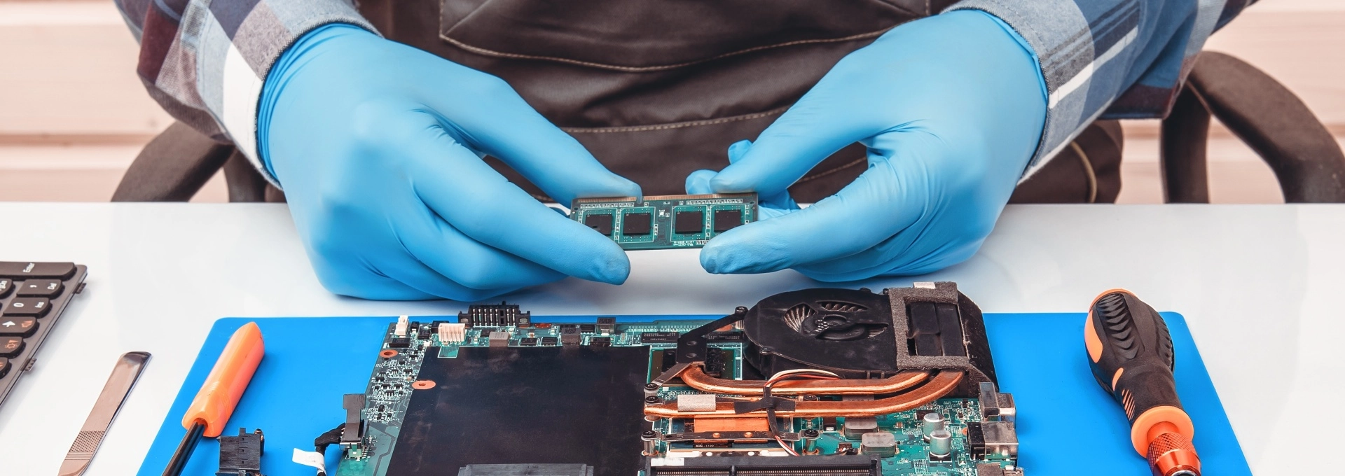
Effective semiconductor repair begins with accurate diagnosis. Modern diagnostic techniques leverage advanced imaging and analysis tools to pinpoint issues at the nanoscale level. These methods, used by eumetrys-robotics.com, not only identify problems but also provide crucial insights for targeted repairs, minimizing unnecessary interventions and reducing overall downtime.
Advanced scanning electron microscopy (SEM) for nanoscale defect detection
Scanning Electron Microscopy (SEM) has become an indispensable tool in semiconductor repair diagnostics. By using a focused beam of electrons, SEM can create high-resolution images of surface structures at magnifications up to 1,000,000x. This level of detail allows technicians to identify nanoscale defects that would be invisible to conventional optical microscopes.
SEM’s capabilities extend beyond simple imaging. When combined with Energy Dispersive X-ray Spectroscopy (EDS), it can provide elemental analysis of defects, helping to determine their composition and origin. This information is crucial for developing targeted repair strategies and preventing future failures.
Thermal imaging and infrared spectroscopy in IC failure analysis
Thermal imaging and infrared spectroscopy play vital roles in identifying heat-related issues in integrated circuits (ICs). These techniques can detect hotspots and abnormal temperature distributions that often indicate underlying problems such as short circuits or excessive power consumption.
By using high-sensitivity infrared cameras, technicians can create thermal maps of operating ICs, revealing areas of concern that may not be visible through other inspection methods. This non-invasive approach is particularly valuable for diagnosing issues in complex, multi-layer chip designs where traditional probing techniques may be impractical or risk damaging the device.
Automated optical inspection (AOI) systems for High-Volume production
In high-volume semiconductor manufacturing environments, manual inspection is often impractical and prone to human error. Automated Optical Inspection (AOI) systems address this challenge by using advanced machine vision algorithms to rapidly scan and analyze semiconductor wafers and packaged devices.
AOI systems can detect a wide range of defects, including:
- Pattern misalignments
- Contamination particles
- Scratches and cracks
- Solder bridge defects
These systems not only improve inspection speed and accuracy but also provide valuable data for process improvement and quality control. By integrating AOI into the production line, manufacturers can catch defects early, reducing the need for costly rework and improving overall yield.
Time-domain reflectometry (TDR) for signal integrity issues
As semiconductor devices operate at increasingly high frequencies, signal integrity becomes a critical concern. Time-Domain Reflectometry (TDR) is a powerful diagnostic technique for identifying and locating signal integrity issues in high-speed circuits.
TDR works by sending a fast-rise-time pulse down a transmission line and analyzing the reflections that occur due to impedance discontinuities. This allows technicians to pinpoint the exact location of problems such as:
- Impedance mismatches
- Open or short circuits
- Damaged or degraded connectors
By using TDR, repair technicians can quickly identify and resolve signal integrity issues that might otherwise lead to intermittent failures or reduced performance in high-speed semiconductor devices.
Cutting-edge semiconductor repair technologies
Once a fault has been accurately diagnosed, the next challenge is to perform precise, effective repairs. Modern semiconductor repair technologies enable technicians to make modifications and repairs at the nanoscale level, often without the need to replace entire components or devices.
Focused ion beam (FIB) circuit edit and microsurgery
Focused Ion Beam (FIB) technology has revolutionized semiconductor repair by allowing for precise modifications to be made at the circuit level. FIB systems use a beam of ions (typically gallium) to selectively remove or deposit material with nanometer precision.
In circuit edit applications, FIB can be used to:
- Cut and reroute metal interconnects
- Create new vias between layers
- Deposit insulating or conductive materials
- Remove unwanted particles or defects
This level of precision allows for the repair of complex integrated circuits without the need for costly redesigns or complete device replacement. FIB microsurgery can extend the life of semiconductor devices and enable rapid prototyping of design modifications.
Laser-assisted chemical etching for Die-Level repairs
Laser-Assisted Chemical Etching (LACE) combines the precision of laser technology with the selectivity of chemical etching to perform highly controlled material removal in semiconductor repairs. This technique is particularly useful for die-level repairs where traditional mechanical methods might risk damaging surrounding structures.
LACE works by using a laser to locally heat the target area, enhancing the chemical reaction rate of an etchant gas. This allows for:
- Selective removal of damaged or unwanted material
- Creation of precise openings for subsequent repair steps
- Modification of device structures without mechanical stress
The combination of laser precision and chemical selectivity makes LACE an invaluable tool for repairing advanced semiconductor devices with minimal collateral damage.
Atomic layer deposition (ALD) for nanoscale conductor restoration
Atomic Layer Deposition (ALD) is a thin film deposition technique that allows for the creation of uniform, conformal layers with atomic-level precision. In semiconductor repair, ALD is increasingly used for restoring damaged conductors and creating new conductive pathways at the nanoscale.
The key advantages of ALD in semiconductor repair include:
- Ability to create ultra-thin, pinhole-free layers
- Excellent step coverage, even in high-aspect-ratio structures
- Precise control over film thickness and composition
These capabilities make ALD ideal for repairing delicate structures in advanced semiconductor devices, where even nanometer-scale variations can significantly impact performance.
Plasma-enhanced chemical vapor deposition (PECVD) in chip repair
Plasma-Enhanced Chemical Vapor Deposition (PECVD) is a versatile technique that enables the deposition of a wide range of materials at relatively low temperatures. In semiconductor repair, PECVD is often used to deposit insulating or passivation layers, as well as to create new conductive structures.
The plasma enhancement in PECVD allows for:
- Lower deposition temperatures, reducing thermal stress on repaired devices
- Improved film density and adhesion compared to traditional CVD
- Greater control over film properties through plasma parameter adjustment
These attributes make PECVD an essential tool in the repair of modern semiconductor devices, particularly where low-temperature processing is critical to preserve existing structures and functionality.
Optimizing cleanroom environments for semiconductor repair
The success of semiconductor repair operations heavily depends on maintaining an ultra-clean environment. As device features shrink to nanometer scales, even microscopic contaminants can render repairs ineffective or cause additional damage. Optimizing cleanroom conditions is therefore crucial for ensuring consistent, high-quality repairs.
ISO class 3 cleanroom standards for advanced node repairs
For repairs on advanced semiconductor nodes (7nm and below), ISO Class 3 cleanroom standards are often necessary. These environments limit airborne particles to extremely low levels, typically less than 1,000 particles per cubic meter for particles ≥0.1 µm in size.
Maintaining ISO Class 3 conditions requires:
- Sophisticated air filtration and circulation systems
- Stringent protocols for personnel entry and movement
- Regular monitoring and verification of particle counts
While challenging to maintain, these ultra-clean conditions are essential for ensuring the success of nanoscale repairs and modifications.
Electrostatic discharge (ESD) prevention protocols in repair stations
Electrostatic Discharge (ESD) can cause catastrophic damage to sensitive semiconductor devices. Implementing robust ESD prevention protocols is critical in repair environments. This includes:
- Use of ESD-safe workstations and tools
- Proper grounding of personnel and equipment
- Control of humidity levels to reduce static buildup
- Regular testing and verification of ESD protection measures
By rigorously adhering to these protocols, repair facilities can minimize the risk of ESD-related damage during delicate repair procedures.
HEPA and ULPA filtration systems for particle control
High-Efficiency Particulate Air (HEPA) and Ultra-Low Penetration Air (ULPA) filtration systems are the backbone of cleanroom air purification. These advanced filters can remove 99.97% (HEPA) to 99.9995% (ULPA) of particles from the air, creating the ultra-clean environment necessary for semiconductor repair.
Effective implementation of HEPA and ULPA filtration involves:
- Strategic placement of filters to create laminar airflow
- Regular maintenance and replacement of filter elements
- Integration with overall cleanroom design for optimal air circulation
The combination of these filtration technologies with proper cleanroom design ensures that repair technicians can work in an environment virtually free of airborne contaminants.
Implementing predictive maintenance in semiconductor fabrication
Predictive maintenance strategies are transforming the way semiconductor manufacturers approach equipment upkeep and repair. By leveraging advanced analytics and real-time monitoring, fabs can anticipate potential failures before they occur, significantly reducing unplanned downtime and optimizing maintenance schedules.
Machine learning algorithms for early fault detection
Machine learning (ML) algorithms are increasingly being applied to analyze vast amounts of sensor data from semiconductor manufacturing equipment. These algorithms can detect subtle patterns and anomalies that might indicate impending failures, often long before they would be noticeable to human operators.
Key benefits of ML-based fault detection include:
- Early identification of performance degradation
- Reduced false alarms compared to traditional threshold-based monitoring
- Continuous learning and improvement of detection accuracy over time
By implementing ML-powered fault detection systems, semiconductor manufacturers can transition from reactive to proactive maintenance strategies, significantly improving equipment reliability and uptime.
Real-time monitoring with industrial internet of things (IIoT) sensors
The Industrial Internet of Things (IIoT) has enabled the deployment of a vast network of sensors throughout semiconductor fabrication facilities. These sensors provide real-time data on equipment performance, environmental conditions, and process parameters.
IIoT sensors can monitor a wide range of variables, including:
- Temperature and humidity levels
- Vibration and acoustic signatures
- Power consumption and electrical characteristics
- Gas and chemical flow rates
By continuously analyzing this data stream, predictive maintenance systems can identify deviations from normal operating conditions and trigger maintenance actions before failures occur.
Integrating predictive analytics with manufacturing execution systems (MES)
To maximize the impact of predictive maintenance, it’s crucial to integrate predictive analytics capabilities with existing Manufacturing Execution Systems (MES). This integration allows for seamless coordination between maintenance predictions and production scheduling, minimizing disruptions to overall fab operations.
Benefits of MES integration include:
- Automated scheduling of maintenance activities during planned downtime
- Real-time adjustment of production plans based on equipment health predictions
- Improved visibility of maintenance impacts on production KPIs
By creating a unified view of maintenance needs and production requirements, fabs can optimize their operations for maximum efficiency and minimal unplanned downtime.
Quality assurance and reliability testing Post-Repair
After completing semiconductor repairs, rigorous quality assurance and reliability testing are essential to ensure that repaired devices meet or exceed original performance specifications. These testing procedures help validate the effectiveness of repairs and provide confidence in the long-term reliability of repaired components.
Accelerated life testing (ALT) for repaired semiconductor devices
Accelerated Life Testing (ALT) is a crucial technique for evaluating the long-term reliability of repaired semiconductor devices. ALT subjects devices to elevated stress conditions (such as high temperature, humidity, or voltage) to simulate years of normal operation in a compressed timeframe.
Key aspects of ALT for repaired devices include:
- Customized stress conditions based on the specific repair performed
- Comparative testing against non-repaired control samples
- Statistical analysis of failure rates and mechanisms
By conducting thorough ALT, manufacturers can gain confidence in the durability of repairs and identify any potential long-term reliability issues.
Burn-in testing procedures for stress screening
Burn-in testing is a form of stress screening that involves operating devices under elevated temperature and voltage conditions for an extended period. This process helps to identify early-life failures (often called “infant mortality”) that might occur shortly after a repair.
Effective burn-in testing for repaired semiconductors typically involves:
- Customized burn-in profiles based on device type and repair history
- Continuous monitoring of device parameters during the burn-in period
- Post-burn-in functional and parametric testing
By subjecting repaired devices to burn-in testing, manufacturers can weed out potentially unreliable units and ensure that only robust, stable devices are returned to service.
X-ray inspection for internal structure verification
X-ray inspection provides a non-destructive method for verifying the internal structure of repaired semiconductor devices. This technique is particularly valuable for assessing repairs that involve modifications to package internals or die-level structures.
Advanced X-ray inspection systems offer:
- High-resolution 2D and 3D imaging capabilities
- Ability to detect voids, cracks, and misalignments
- Comparison against “golden sample” reference images
By incorporating X-ray inspection into post-repair quality assurance procedures, manufacturers can verify the structural integrity of repairs and detect any internal anomalies that might affect device reliability.
Electrical parametric testing and characterization
Comprehensive electrical parametric testing is essential for ensuring that repaired semiconductor devices meet all functional and performance specifications. This testing often involves a combination of DC and AC measurements across a range of operating conditions.
Key aspects of post-repair electrical testing include:
- Comprehensive DC and AC parametric measurements
- Testing across temperature and voltage corners
- Comparison against pre-repair baseline measurements
- Evaluation of key performance indicators specific to the device type
By conducting thorough electrical characterization, manufacturers can verify that repaired devices not only function correctly but also meet all performance specifications required for their intended application. This final step in the quality assurance process helps ensure that repaired semiconductors can be confidently returned to service with minimal risk of field failures.